Surface mount technology (SMT) PCBA processes involve three essential steps: solder paste printing, component placement, and reflow soldering. These steps directly influence the quality and reliability of your SMT PCBA assemblies. You need to pay close attention to each process because:
- The quality of solder paste printing determines the strength and consistency of solder joints in SMT PCBA.
- Accurate component placement prevents misalignment, which can cause up to 60% of defects in SMT PCBA assemblies.
- Precise reflow soldering ensures proper joint formation and reduces costly rework in SMT PCBA.
Inspection and best practices at every stage help you achieve reliable results for your PCB projects.
Mastering SMT PCBA: A Technical Guide to Printing, Placement, and Reflow Soldering
- Understand the three key steps in SMT PCBA: solder paste printing, component placement, and reflow soldering. Each step is crucial for ensuring quality and reliability.
- Implement Solder Paste Inspection (SPI) to catch defects early. This proactive measure can reduce soldering issues by up to 70%, saving time and costs.
- Use advanced placement equipment to ensure precise component mounting. High-speed machines can handle thousands of components per hour, improving efficiency.
- Control the reflow temperature profile carefully. Proper temperature management prevents defects and ensures strong solder joints.
- Integrate inspection systems like Automated Optical Inspection (AOI) at every stage. This helps maintain high quality and reduces the risk of costly failures.
SMT Solder Paste Printing

Process Overview
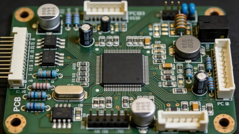
Solder paste printing marks the first critical step in the SMT process flow. You apply solder paste to the pcb pads using a stencil, which acts as a precise mask. This process ensures that each pad receives the correct amount of solder paste, setting the foundation for reliable pcba assembly. Accurate positioning and volume control prevent issues such as short circuits or poor wetting of components. During reflow soldering, the solder paste melts and forms a strong bond between the pcb and surface-mounted devices. The success of your SMT PCBAs depends on the quality of this initial printing step.
Tip: Consistent solder paste application reduces the risk of defects later in the process.
Stencil and Paste Selection
Stencil tension plays a vital role in achieving accurate solder paste deposition. You need to maintain high tension, especially when working with ultra-fine-pitch components. Higher stencil tension improves paste transfer and reduces the chance of insufficient solder volume. The condition of the stencil foil, including wear and deformation, also affects print quality.
When selecting solder paste, you must consider several factors. The table below outlines key criteria for choosing the right paste for your surface mount technology application. Lead-free SAC305 is a popular choice for high-reliability assemblies, offering excellent performance in automotive and medical environments.
| Selection Factor | Primary Consideration | Impact on Solder Paste Choice |
|---|---|---|
| Product Reliability | End-use environment (Automotive, Medical, Consumer) | High-reliability parts demand superior alloys (e.g., SAC305) and water-soluble flux for residue removal. |
| Component Pitch / Size | Smallest component size or tightest pitch | Smaller particle size (T4 or T5) needed for high-resolution printing and to minimize solder balling. |
| Heat Sensitivity | Low-temperature-tolerant devices (LEDs, connectors) | Use Low-Temperature Solder Paste to keep the reflow oven peak below 180°C. |
| Cleaning Capability | Availability of cleaning equipment | No-Clean paste for limited washing; Water-Soluble paste for highest cleanliness. |
| Reflow Profile | Temperature capacity of pcb and components | Alloy melting point must match the safe reflow temperature window. |
Solder Paste Inspection (SPI)
Solder Paste Inspection (SPI) is essential for quality control in SMT. You use SPI systems to detect defects immediately after printing, before placement and reflow oven stages. Up to 70% of soldering defects originate from improper solder paste application, making early inspection crucial. SPI identifies issues such as solder bridging, solder balls, insufficient solder, paste slump, misalignment, and stencil clogging.
| Defect Type | Causes | Impact |
|---|---|---|
| Solder Bridging | Excess paste, poor stencil alignment, inadequate pad separation, and humidity | Electrical shorts, circuit failure, unreliable performance |
| Solder Balls | Excess moisture, inconsistent pressure, improper reflow, oxidation | Unintended connections, risk of shorts or intermittent failures |
| Insufficient Solder | Undersized apertures, worn stencils, incorrect pressure, and paste degradation | Weak joints, possible failure under stress or thermal cycling |
| Solder Paste Slump | Low viscosity, excessive volume, delayed reflow, poor stencil contact | Bridging or insufficient solder in critical areas |
| Misalignment | Inaccurate stencil alignment, vibration, and inconsistent pcb flatness | Open circuits, weak joints, need for manual rework |
| Stencil Clogging | Insufficient cleaning, low-quality paste, small apertures, poor storage | Incomplete or missing deposits, potential open circuits |
Note: The introduction of SPI shifts your quality control from reactive to proactive. You can catch and correct defects early, reducing costly rework and improving overall yield.
Solder paste inspection ensures that only boards with properly deposited solder paste move forward in the SMT process flow. This step protects the integrity of your pcb assembly and supports reliable pick and place operations.
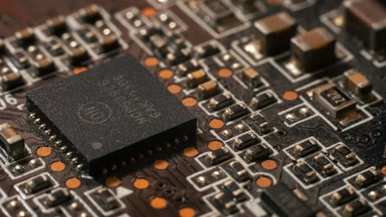
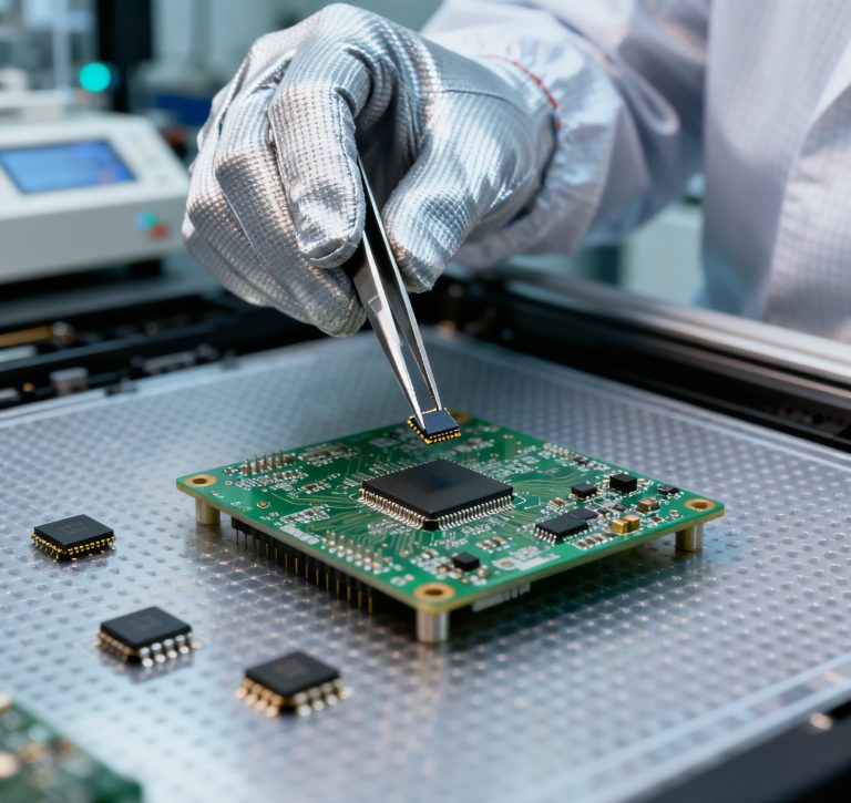
Component Placement in SMT PCBA

Placement Equipment
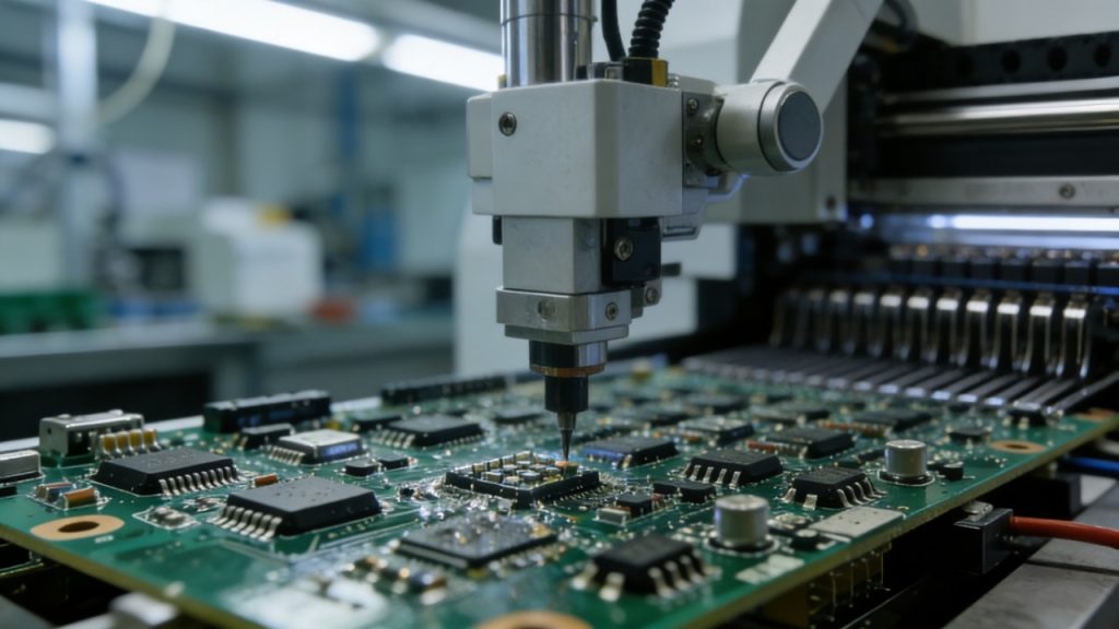
You rely on advanced placement equipment to achieve precise and efficient component mounting in the SMT PCBAs process. Pick-and-place machines serve as the backbone of modern SMT lines, handling thousands of components per hour with remarkable accuracy. These machines use robotic arms and vision systems to identify, pick, and position surface-mount devices onto the PCBA. For high-volume production, automatic pick-and-place and turret-type machines deliver speeds exceeding 50,000 components per hour (CPH), making them ideal for dense pcb assembly.
| Equipment Type | Description | Placement Speed (CPH) |
|---|---|---|
| Automatic Pick-and-Place | Fully automated machines for high-speed, high-volume assembly. | >50,000 |
| Turret-type | High-speed model with multiple heads for simultaneous operations. | >50,000 |
| Solder Paste Printing Machines | Applies solder paste to PCB pads for component placement. | N/A |
| Reflow Soldering Machines | Melts solder paste to bond components to the PCB. | N/A |
Tip: Choose placement equipment that matches your production volume and component complexity. High-speed machines reduce cycle time and support high-density layouts.
Precision and Density
Precision in component placement drives the quality of your SMT process flow. You must maintain tight tolerances, especially when working with fine-pitch components such as 0201 or 01005 packages. Even a 0.1 mm misalignment can cause defects like tombstoning or skewing, which compromise the reliability of your pcb assembly. Fiducial marks on the pcb help your machines align components accurately, minimizing errors in high-density designs.
- Placement accuracy prevents misalignment and reduces defect rates.
- High-density boards require advanced vision systems and calibration to handle small components.
- Errors in placement can disrupt connections and lead to costly rework.
Note: Use fiducial marks and regular machine calibration to maintain placement precision. Advanced systems help you achieve consistent results, even with challenging layouts.
Quality Factors
You face several challenges during the component placement stage of SMT PCBA. Precision issues arise when machines misplace components by fractions of a millimeter, especially with fine-pitch devices. High-speed production sometimes sacrifices accuracy, increasing the risk of defects. A mix of SMT and through-hole components complicates handling and requires different mounting techniques. Poor machine calibration leads to consistent errors, while tight tolerance limits demand advanced equipment.
| Challenge | Description |
|---|---|
| Ensuring Component Placement Accuracy | Accurate placement is crucial; misalignment can lead to short circuits or reduced performance. |
| Achieving Consistent Solder Paste Application | Inconsistent application can cause weak joints and defects like tombstoning and bridging. |
| Optimizing the Reflow Soldering Process | Incorrect profiles can lead to cold joints or heat damage. |
| Managing Component Variability | Variations in size and shape complicate assembly, leading to errors. |
| Preventing PCB Warpage | Warpage can cause misalignments and poor solder joints, especially in large or thin boards. |
| Mitigating Electrostatic Discharge (ESD) | ESD can damage sensitive components during handling, leading to failures. |
| Enhancing Inspection and Quality Control | Early defect identification is crucial to prevent costly rework or failures in the field. |
You ensure reliability by using automated optical inspection (AOI) and x-ray inspection. AOI systems scan each pcb for misaligned components and visual defects, while X-ray inspection checks hidden solder joints in high-density assemblies. Solder paste inspection (SPI) verifies correct paste application before placement, reducing the risk of defects.
- Automated optical inspection detects misalignment and visual flaws early.
- X-ray inspection identifies hidden soldering issues in complex assemblies.
- Solder paste inspection confirms proper paste volume and alignment.
Tip: Integrate inspection systems at every stage of the SMT process flow. Early detection of placement errors improves yield and reduces rework.
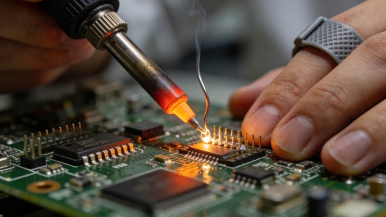
Surface Mount Technology Reflow Soldering
Reflow Process Steps
You must understand the four main stages of the reflow soldering process to achieve reliable connections in your pcb assembly. Each stage plays a unique role in the SMT process flow:
| Stage | Purpose |
|---|---|
| Preheat | Gradually heats the pcb to avoid thermal shock and activates the flux. |
| Soak | Maintains a stable temperature for equalization and further flux activation. |
| Reflow | Melts the solder paste, forming strong joints between components and pads. |
| Cooling | Solidifies the solder, minimizing thermal stress and ensuring robust connections. |
You start with preheat, which raises the temperature slowly to prevent damage and activate the flux. The soak stage holds the pcb at a steady temperature, allowing heat to distribute evenly and the flux to clean the surfaces. During reflow, the solder paste melts and creates the electrical and mechanical bonds. The cooling stage then solidifies the solder, locking in the connections and preventing cracks.
Temperature Profile
You need to control the temperature profile carefully during reflow soldering. This profile determines how the solder melts and solidifies, directly affecting joint quality. If you exceed a peak temperature of 260°C or keep the time above liquidus (TAL) longer than 120 seconds, you risk excessive intermetallic compound growth, which weakens the joints. Insufficient wetting can occur if the temperature is too low or the TAL is too short. For lead-free solder, you should target a peak between 235°C and 250°C, with a TAL of 60–90 seconds.
| Stage | Leaded Solder (SnPb) | Lead-Free Solder (SAC) |
|---|---|---|
| Preheat | 120–150 °C | 150–180 °C |
| Soak | 150–180 °C | 170–190 °C |
| Peak | 205–220 °C | 235–250 °C |
| Cooling Rate | 3–6 °C/s | 3–6 °C/s |
You must monitor each zone to avoid defects like tombstoning and insufficient wetting. Proper cooling rates prevent cracks and limit unwanted grain growth in the solder joint. This attention to detail ensures your SMT PCBA meets industry standards for durability and performance.
Post-Reflow Inspection (AOI)
After reflow, you rely on automated optical inspection (AOI) to verify solder joint quality. AOI systems scan each pcb for surface defects, including solder bridges, insufficient solder, tombstoning, and open joints. These machines detect over 95% of surface issues, making them essential for quality assurance in the SMT process flow.
- AOI identifies soldering defects before the boards move to the next production step.
- You can catch problems early, reducing rework and improving overall yield.
- AOI ensures your pcb assembly meets reliability standards for high-performance applications.
Tip: Integrate AOI after reflow to maintain high quality and reduce costly failures in your finished products.
Integrating SMT PCBA Processes
Workflow Connection
You need to understand how each step in the SMT PCBAs workflow connects to create a seamless process. The SMT process flow starts with solder paste application, which forms a temporary adhesive layer on the PCBA. Automated machines then place components onto the solder-pasted pcb with high precision. The PCBA moves into the reflow soldering oven, where the solder paste melts and forms permanent joints. Inspection follows, ensuring the pcb assembly meets strict quality standards. Some assemblies require through-hole components, which use a different soldering method,d such as wave soldering. After assembly, you perform functional testing, cleaning, coating, and final inspection to guarantee reliability before shipping.
| Step | Description |
|---|---|
| Solder Paste | The application creates a temporary adhesive layer on the pcb. |
| Component Placement | Automated machines accurately place components on the solder-pasted pcb. |
| Reflow Soldering | The PCBA passes through a reflow oven to melt the solder paste and form joints. |
| Inspection | Ensures the pcb meets quality and functional standards. |
| Through-Hole | Wave soldering method for components needing stronger connections. |
| Post-Assembly | Functional testing, cleaning, coating, and final inspection. |
Tip: Each process step directly affects the next. Early detection of defects prevents costly rework and improves overall yield.
Impact on Quality
You achieve high product quality by integrating each process step and focusing on design for manufacturability. This approach reduces errors and streamlines production. SMT allows you to build smaller, more complex circuits, which are essential for modern technology. Automation in SMT reduces human error and ensures consistent quality. You benefit from higher yields and fewer revisions when you implement a strong DFM strategy.
- SMT streamlines manufacturing and boosts reliability.
- You produce advanced circuits for modern devices.
- Automation supports consistent quality and reduces mistakes.
- Effective DFM minimizes errors and production issues.
- Thoughtful design reduces revisions and smooths the transition from design to assembly.
- Strong DFM leads to higher yield and fewer costly rework cycles.
Note: Sanshun Smart uses advanced SPI and AOI equipment at every stage to ensure zero defects and maintain the highest standards in pcb assembly.
Quality Control Measures
You must apply rigorous quality control at every stage of the SMT process flow. Inspection methods include incoming quality control, bare board inspection, solder paste inspection, automated optical inspection, automated x-ray inspection, functional testing, and in-circuit testing. Each method targets specific risks and ensures your PCBA meets all requirements.
| Inspection Method | Purpose | Impact |
|---|---|---|
| Incoming Quality Control | Verifies MSL, checks dry pack seals | Minimizes risk of counterfeit parts |
| Bare Board Inspection | Detects surface defects, checks dimensions | Ensures mechanical compatibility |
| Solder Paste Inspection | Checks solder paste volume, height, and area | Prevents soldering issues |
| Automated Optical Inspection (AOI) | Identifies placement and solder joint defects | Ensures quality assurance |
| Automated X-ray Inspection (AXI) | Examines hidden solder joints | Detects internal defects |
| Functional Testing (FCT) | Verifies overall board performance | Confirms design specifications |
| In-Circuit Testing (ICT) | Tests individual components | Locates opens/shorts quickly |
- Solder Paste Inspection ensures correct application.
- AOI detects surface defects and verifies placement.
- Functional Testing confirms board operation.
- In-Circuit Testing checks individual components.
Tip: You improve reliability and reduce defects by integrating inspection systems such as SPI and AOI throughout the SMT PCBA process.
SMT Best Practices and Tips
Optimizing Printing
You improve solder paste printing by following strict process controls. Check the manufacturer’s specifications for solder paste viscosity, aiming for 800 to 1200 Pa·s. Use automated inspection systems such as 2D or 3D SPI to measure paste volume and alignment. This step can reduce defects by up to 70%. Maintain a controlled environment with a temperature between 20°C and 25°C and humidity from 40% to 60%. Clean stencils after every 5 to 10 prints to prevent paste buildup. Adjust squeegee pressure and print speed for even application. Design stencil apertures and thickness to match your pcb assembly needs.
- Monitor solder paste viscosity.
- Use SPI for early defect detection.
- Control temperature and humidity.
- Clean stencils regularly.
Improving Placement
You achieve accurate component placement by optimizing machine setup and feeder selection. Choose high-quality, laser-cut stencils for fine-pitch components. Monitor paste storage conditions, keeping the temperature between 2°C and 10°C. Calibrate pick-and-place machines and select suitable heads for each component type. The table below summarizes key placement techniques:
| Technique | Description |
|---|---|
| High-quality stencils | Laser-cut for fine-pitch accuracy (down to 0.4 mm pitch). |
| Regular cleaning | Prevents uneven deposits and misalignment. |
| Paste monitoring | Ensures ideal viscosity and storage conditions. |
- Optimize placement parameters for each SMT process flow.
- Use AOI to verify alignment and catch errors early.
Perfecting Reflow
You minimize defects during reflow by controlling the temperature profile and stencil design. Optimize stencil apertures to 80–90% of pad size and use a thickness of 0.1–0.15 mm for fine-pitch components. Adjust the reflow profile with a gradual ramp-up rate of 1–3°C per second in the preheat zone. Balance the soak region temperature between 150°C and 180°C for 60–90 seconds. Use a solder alloy with a larger pasty range, such as SAC305, to reduce tombstoning. Verify solder paste deposition with SPI tools before reflow.
- Optimize stencil design and thickness.
- Control ramp-up and soak temperatures.
- Use suitable solder alloys for reliability.
- Calibrate machines for precise placement.
Avoiding Common Defects
You prevent defects in SMT PCBAs by focusing on process control and material management. Solder balls result from excess moisture or rapid heating. Prevent these by proper storage and a suitable preheat phase. Tombstoning occurs due to uneven heating; avoid this with a symmetrical reflow profile. Component misalignment stems from poor calibration; regular calibration and AOI help prevent this. Solder voids arise from trapped moisture; optimize the reflow profile and bake components. Lifted leads and de-wetting result from improper handling and contamination; maintain strict cleanliness protocols.
- Store components and paste correctly.
- Calibrate machines and inspect regularly.
- Optimize reflow profiles for each soldering method.
- Use solder mask and align stencils to prevent solder bridges.
You increase first-pass yield rates and long-term reliability by following these best practices throughout the SMT process flow. Higher solder paste volumes and optimized soldering methods support strong joints, especially for high-reliability applications.
You achieve high-quality electronics manufacturing when you master each step of the SMT PCBAs process. Inspection at every stage, from solder paste printing to final automated optical inspection, ensures your printed circuit board meets strict standards. The table below highlights strategies that improve pcb assembly quality:
| Strategy | Description |
|---|---|
| SMT Line Optimization | Enhances efficiency and targets OEE rates above 85%. |
| Lean Manufacturing | Streamlines workflows and eliminates waste. |
| Advanced Equipment | Boosts first-pass yields and reduces errors. |
Granular inspections and functional testing confirm reliability. Looking for a reliable PCBA partner with high-precision SMT lines? Contact Sanshun Smart for a DFM review today.
FAQ
What is the main advantage of SMT over traditional through-hole assembly?
You achieve higher component density and faster production with SMT. SMT allows you to mount components directly onto the PCB surface, which saves space and supports miniaturization.
How do you prevent soldering defects during SMT PCBA?
You control solder paste volume, maintain stencil cleanliness, and monitor reflow temperature profiles. Automated inspection systems like SPI and AOI help you catch defects early.
Why is automated optical inspection (AOI) important in SMT?
AOI helps you detect placement and soldering errors quickly. You improve yield and reduce manual rework by using AOI after both placement and reflow stages.
What factors affect component placement accuracy?
You must calibrate pick-and-place machines, use fiducial marks, and select high-quality stencils. Environmental controls and regular equipment maintenance also improve placement precision.
Can you use SMT for all types of electronic components?
You use SMT for most components, but some connectors, switches, and large parts still require through-hole mounting for mechanical strength.