You often encounter SMT PCBA defects like solder bridging, tombstoning, solder balls, insufficient solder, missing components, cold solder joints, misalignment, and open joints in PCBA assembly. These issues directly impact product reliability and yield. The table below presents recent industry statistics, highlighting the prevalence of open solder joints, solder shorts, and component misalignment:
| Defect Type | Percentage | Description |
|---|---|---|
| Open Solder Joints | 35% | The joint appears soldered but lacks a proper connection. |
| Solder Shorts | 20% | Unintended connections between adjacent pins. |
| Component Misalignment | 20% | Components not aligned with PCB pads. |

Process control and advanced inspection, such as AOI and X-ray, play a vital role in reducing these defects. As a senior QA manager at Sanshun Smart, I have seen how rigorous quality management ensures reliable outcomes. You will find a troubleshooting table and best practices for quick reference.
Zero-Defect SMT PCBA: Professional Strategies for Preventing Common Assembly Failures
- SMT PCBA defects like solder bridging and tombstoning can severely impact product reliability. Understanding these defects is crucial for manufacturers.
- Implementing strict process controls and advanced inspection methods, such as AOI and X-ray, significantly reduces defect rates and improves quality.
- Regular calibration of equipment ensures accurate component placement and consistent solder paste application, preventing common defects.
- Conducting Design for Manufacturability (DFM) checks early in the design phase helps avoid layout issues that lead to defects.
- Continuous improvement through training and technology adoption fosters a culture of quality awareness, enhancing overall assembly performance.
SMT PCBA Defects Overview
What Are SMT PCBA Defects?
You encounter smt pcba defects when the assembly process produces unintended electrical or mechanical issues on the circuit board. These issues can range from minor cosmetic flaws to critical failures that compromise the entire product. In my experience, you should pay close attention to the following common SMT defects:
- Solder bridging (shorts): Unintended connections between adjacent conductors due to excessive solder.
- Tombstoning: Small chip components stand upright because of uneven heating or solder paste volume.
- Insufficient solder or open joints: Weak or missing connections caused by too little solder paste.
- Solder balls and beading: Small particles form from moisture contamination or too much solder paste.
- Cold solder joints: Dull, grainy joints that signal poor bonding from inadequate heat.
- Voids in solder joints: Air pockets inside the joint, often from trapped flux.
- HiP defect: BGA solder balls detach from pads due to warpage or oxidation.
- Component misalignment: Incorrect placement due to machine inaccuracy.
These defects can introduce solder bridges, open circuits, and misaligned components, all of which reduce the performance and lifespan of your electronic products.
Why Defects Occur
You often see defects arise from a combination of process, material, and equipment factors. The most frequent causes include:
- Shorts (solder bridging) occur when solder connects one lead to another, risking serious damage.
- Component shift or misalignment happens during reflow, as components float on molten solder.
- Missing components result from vacuum system failure, incorrect feeder setup, or insufficient solder paste.
- Tombstoning develops when uneven wetting forces cause one end of a component to lift.
- Solder beading stems from excessive solder paste or flux outgassing during preheat.
- Insufficient fills come from blocked stencil apertures or improper squeegee pressure.
You must address these root causes to maintain high assembly quality. At Sanshun Smart, we implement strict process controls and advanced inspection to minimize common SMT defects and ensure reliable outcomes for every project.
Common SMT Defects and Causes
Solder Bridging
You often encounter solder bridging when excess solder forms an unintended connection between adjacent pads or component leads. This defect creates electrical shorts, which can cause device malfunction or catastrophic failure. Bridging results from several process issues:
- Excessive solder paste deposition during stencil printing.
- Poor stencil design, such as oversized apertures or insufficient gasketing.
- Misalignment of the stencil or PCB during printing.
- Inaccurate component placement, which can smear solder paste across pads.
- Improper reflow profiles that fail to control solder flow.
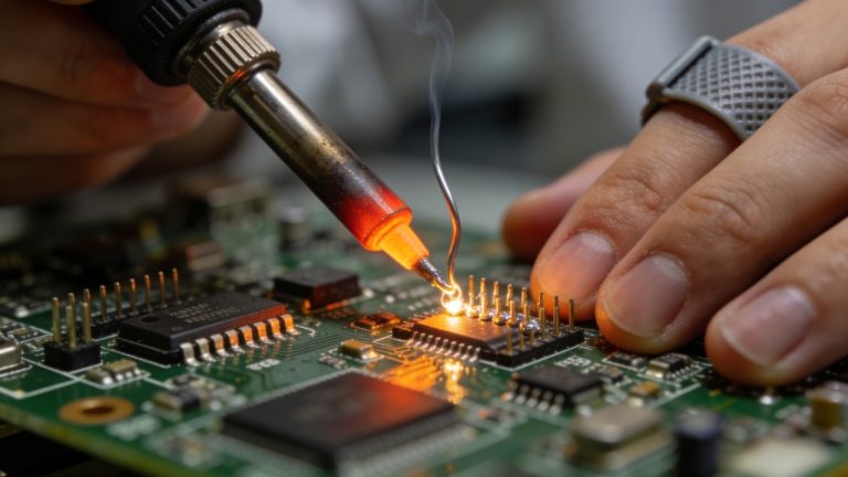
You must monitor bridging closely because it can occur at any stage, from paste printing to reflow. In my experience, you can reduce solder bridging by optimizing stencil design, maintaining precise alignment, and calibrating reflow oven profiles. Automated Optical Inspection (AOI) systems help you detect bridging early, preventing defective boards from reaching final assembly.
Tip: Regularly inspect your stencils for wear and clean them to prevent bridging caused by paste buildup.
Tombstoning
Tombstoning occurs when a small chip component, such as a resistor or capacitor, stands upright on one end during reflow. This defect breaks the electrical connection and renders the component nonfunctional. You see tombstoning most often with 0402 or 0603 chips due to their small size and low mass.
The main causes of tombstoning include:
| Factor | Description |
|---|---|
| Thermal Imbalances | Uneven temperature distribution can cause one side of a component to lift off its pad during soldering. |
| Improper Pad Design | Asymmetric pads can lead to unequal solder application, causing one side to have more solder than the other. |
| Solder Paste Application | Inconsistent solder paste application can create wetting imbalances, leading to tombstoning. |
| Incorrect PNP Placement | Mismatches in placement can result in insufficient solder on one side, causing liftoff. |
| Bad Reflow Oven Regulation | Uneven heating in the reflow oven can lead to uneven wetting and contribute to tombstoning. |
| PCB Contamination | Contaminants can prevent proper solder bonding, leading to poor solder joint formation. |
| Board Warpage | Warpage can create uneven thermal conditions, affecting solder melting and causing tombstoning. |
You must pay special attention to pad design and solder paste volume. Uneven heating profiles and contamination also increase the risk of tombstoning. You can minimize this defect by ensuring symmetric pad layouts, consistent solder paste application, and precise reflow oven regulation. AOI systems and X-ray inspection help you catch tombstoning early in the process.
Solder Balls
Solder balls are small, spherical particles of solder that appear around pads or between component leads after reflow. These particles can cause shorts or reliability issues if they detach and migrate. You often see solder balls when process parameters are not tightly controlled.
The most common causes of solder balls include:
- Improper reflow temperature settings, which cause moisture in solder paste to boil and spatter solder.
- Poor stencil design, resulting in incomplete or excessive solder paste deposits.
- Extended time between paste printing and reflow, leading to oxidation of solder particles.
- Excessive pressure during component mounting, which squeezes solder paste out from under components.
- Inadequate cleaning of PCBs, leaving residual solder paste that forms balls during reflow.
- Insufficient wetting between component pins and pads, causing solder to flow out and bead up.
You can prevent solder balls by optimizing reflow profiles, using high-quality solder paste, and maintaining clean PCB surfaces. Regular stencil inspection and cleaning also reduces the risk of this defect.
Insufficient Solder
Insufficient solder is one of the most prevalent defects in SMT PCBAs. You recognize this defect by weak or incomplete solder joints, which compromise both electrical conductivity and mechanical strength. Insufficient solder can lead to open circuits, intermittent connections, or even voids in solder joints.
Typical causes of insufficient solder include:
- Inadequate solder paste deposition due to stencil misalignment or clogged apertures.
- Poor wetting of pads or component leads, often from contamination or oxidation.
- Improper reflow profiles that do not allow solder to fully melt and flow.
- Component warpage, which lifts leads off pads and prevents proper soldering.
You can address insufficient solder by optimizing stencil design for correct paste volume, ensuring clean and well-finished pads, and fine-tuning reflow profiles. Regular maintenance of printing equipment and careful monitoring of solder paste condition also help you minimize this defect.
Note: Insufficient solder not only weakens joints but also increases the risk of voids, which can further degrade reliability.
Missing Components
Missing components occur when parts fail to be placed on the PCB during assembly. You often trace this defect to issues with solder paste properties, placement machine calibration, or handling errors.
Common causes include:
- Use of solder paste beyond its recommended period reduces tackiness and causes components to shift or fall off.
- Low viscosity of solder paste, which fails to hold components in place during transport or reflow.
- Excessive flux content in solder paste leads to component displacement during heating.
- Vibration or improper handling after placement, which can dislodge components.
- Inadequate adjustment of the placement nozzle air pressure results in poor pick-and-place performance.
- Mechanical faults in the placement machine are causing misplacement or omission of components.
You can reduce missing components by using fresh solder paste, calibrating placement equipment, and ensuring proper handling throughout the process.
Cold Solder Joints
Cold solder joints are among the most common soldering defects, especially in environments with poor process control. You identify cold solder joints by their dull, grainy appearance and weak mechanical strength. These joints often result in intermittent or failed electrical connections.
Leading causes of cold solder joints include:
- Insufficient heat during reflow prevents solder from fully melting and bonding.
- Contaminated surfaces, such as oxidized pads or leads, inhibit solder adhesion.
- Poor flux application, which fails to prepare surfaces for soldering.
- Use of incorrect or impure solder alloys results in unreliable joints.
You can prevent cold solder joints by maintaining proper reflow temperatures, cleaning all surfaces thoroughly, and using high-quality flux and solder alloys. Automated inspection systems help you detect these defects before final assembly.
Component Misalignment
Component misalignment remains a significant source of defects in SMT assembly. Placement errors account for up to 60% of all defects, making alignment critical for high-quality production.
Key factors contributing to misalignment include:
| Factor Type | Description |
|---|---|
| Material-Related | Dimensional tolerances, shape irregularities, warped boards, and surface contamination can hinder alignment. |
| Process-Related | Incorrect process settings, placement pressure, excessive speed, and programming errors can lead to misalignment. |
| Environmental Factors | Temperature fluctuations, humidity, and dust can affect the stability and alignment of components. |
You can minimize misalignment by controlling material quality, optimizing placement machine settings, and maintaining a clean, stable production environment.
Open Joints
Open joints occur when a solder joint appears complete but lacks a true electrical connection. You often find this defect in high-density assemblies or with fine-pitch components. Causes include insufficient solder, poor wetting, or contamination. Open joints can lead to intermittent failures or total loss of function.
You can prevent open joints by ensuring proper solder paste volume, maintaining clean surfaces, and verifying reflow profiles. AOI and X-ray inspection help you detect open joints that are not visible to the naked eye.
Remember: Open joints and voids both compromise reliability, but open joints are especially dangerous because they may pass initial testing and fail later in the field.
Prevention Methods in SMT PCBA
Process Control Measures
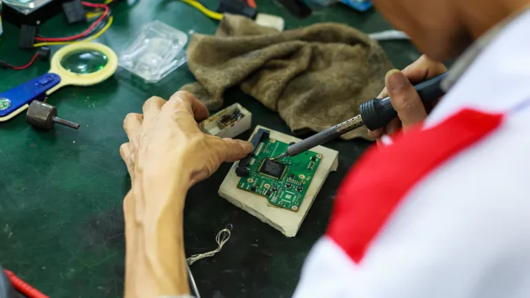
You must implement strict process control to reduce defects in SMT PCBAs. Start with PCB quality control by inspecting every batch for deformation, oxidation, and scratches. Monitor solder paste application and storage by checking validity, temperature, and humidity. During solder paste printing, ensure complete coverage, even thickness, and no bridging. For mounting, use accurate programming and debug chip mounters. Analyze chip mounting sequences and clarify defect positions. Set proper reflow soldering temperature curves and avoid vibration. After reflow, inspect for smooth solder joints and the absence of residues. These steps form the backbone of quality control in pcba assembly.
| Process Control Measure | Description |
|---|---|
| PCB Quality Control | Inspect all batches for deformation, oxidation, scratches, and even printing. |
| Application and Storage of Solder Paste | Monitor validity, control temperature/humidity, and manage mixing ratios. |
| Solder Paste Printing Control | Ensure complete printing, no bridging, and even thickness. |
| Mounting Requirement | Use correct SMDs, accurate programming, and proper debugging. |
| Chip Mounting Defect Solutions | Analyze sequences, clarify defect positions, and study redundancy. |
| Reflow Soldering Requirements | Set temperature curves, avoid vibration, and control metal oxide content. |
| Inspection After Reflow | Check for complete soldering, smooth surfaces, and no residues. |
AOI and SPI Inspection
You rely on AOI and SPI systems to catch defects early. SPI (Solder Paste Inspection) checks solder paste volume and placement before mounting. AOI (Automated Optical Inspection) scans for solder bridging, missing components, and misalignment after placement and reflow. SPI reduces PCB failure rates by over 85% and cuts rework costs by more than 90%. Since 75% of defects come from poor solder paste printing, SPI intercepts these issues, ensuring high-quality solder paste printing and reducing defects in finished products. AOI logic uses high-resolution cameras and pattern recognition to flag anomalies, supporting robust inspection and quality assurance.
| Evidence | Impact |
|---|---|
| SPI reduces PCB failure rate by over 85% | Significant reduction in rework and scrap costs by more than 90% |
| 75% of defects in SMT are due to poor solder paste printing | SPI intercepts these defects, leading to better quality control |
| SPI ensures high-quality solder paste printing | Reduces potential defects in finished products significantly |
X-Ray for Hidden Defects
You cannot detect all defects visually. X-ray inspection becomes essential, especially for BGAs and fine-pitch components. X-ray inspection reveals voids, cracks, inclusions, porosity, component placement errors, solder joint defects, and foreign object debris. You use this technology to ensure hidden solder joints meet reliability standards and to catch issues that AOI cannot see.
| Defect Type | Description |
|---|---|
| Voids | Empty spaces or air pockets inside a material or component that weaken structural integrity. |
| Cracks | Ruptures or tears within a material caused by stresses or thermal cycling, detectable by X-ray. |
| Inclusions | Foreign particles embedded within a material can affect performance. |
| Porosity | Small, self-connected voids diminish strength and durability. |
| Component Placement Errors | Misplacement of components on PCBs can lead to performance issues. |
| Solder Joint Defects | Issues in solder joints, such as cold solder joints or insufficient solder, are detectable by X-ray. |
| Foreign Object Debris (FOD) | Undesirable materials that can cause short circuits or contamination problems. |
Equipment Calibration
You must calibrate all equipment regularly to prevent defects. Calibrate pick-and-place machines for accurate component placement. Adjust stencil printers to maintain consistent solder paste deposition and avoid clogging. Set reflow ovens to maintain proper temperature profiles, which prevent thermal defects and support reflow soldering optimization.
| Calibration Type | Impact on Defect Prevention |
|---|---|
| Pick-and-Place Machines | Ensures accurate component placement, reducing misplacement. |
| Stencil Printer | Maintains consistent solder paste deposition, avoiding clogging. |
| Reflow Oven | Maintains proper temperature profiles, preventing thermal defects. |
DFM and Reflow Profiling
You should conduct Design for Manufacturability (DFM) checks early in the design phase. DFM reviews help you avoid layout issues that lead to open joints or solder bridging. Reflow profiling ensures the solder melts and solidifies correctly, preventing cold solder joints and tombstoning. You must optimize reflow soldering parameters for each board type to achieve consistent results.
Troubleshooting Table
You can use the following table for quick reference when troubleshooting common SMT PCBA defects:
| Defect | Troubleshooting Step |
|---|---|
| Solder Bridging | Adjust stencil design, reduce solder paste, optimize reflow profile, and inspect for misalignment. |
| Tombstoning | Balance pad design, ensure even solder paste, regulate reflow temperature, and clean PCBA surfaces. |
| Solder Balls | Use fresh solder paste, clean PCBs, optimize reflow, and inspect the stencil for wear. |
| Insufficient Solder | Check stencil apertures, clean pads, adjust paste volume, and verify reflow profile. |
| Missing Components | Use fresh solder paste, calibrate the placement machine, check nozzle pressure, and handle boards carefully. |
| Cold Solder Joints | Increase reflow temperature, clean surfaces, use quality flux, and inspect for oxidation. |
| Component Misalignment | Calibrate placement machine, control environment, inspect material quality, and adjust process settings. |
| Open Joints | Increase solder paste, clean surfaces, verify reflow profile, use AOI, and x-ray inspection. |
Tip: Combine AOI, SPI, and x-ray inspection with robust process control for the highest level of inspection and quality assurance in SMT PCBA.
You achieve reliable SMT PCBA assemblies by prioritizing proactive defect prevention and continuous improvement. Advanced technology, strict quality control, and comprehensive training programs drive defect reduction and accuracy:
| Benefit | Description |
|---|---|
| Advanced Technology | State-of-the-art equipment ensures high accuracy and speed in placement. |
| Quality Control | Rigorous inspections and testing prevent defects before they occur. |
| Training Programs | Skilled operators foster a culture of quality awareness. |
Continuous improvement strengthens your process:
- Master SMT reflow soldering to reduce cold joints and shifting.
- Use AOI and ICT for robust quality assurance.
- Optimize process flows and adopt advanced detection technologies.
You build high-performance assemblies by combining inspection, process control, and design best practices. Sanshun Smart delivers consistent quality and reliability in every PCBA project.
FAQ
What is the most common SMT PCBA defect you see in manufacturing?
You most often encounter open solder joints and solder bridging. These defects can cause electrical failures and reduce product reliability. You must use advanced inspection and strict process control to minimize these issues in your SMT PCBA assembly.
How do you prevent solder bridging during SMT assembly?
You should optimize stencil design, control solder paste volume, and calibrate placement machines. AOI systems help you detect solder bridging early. At Sanshun Smart, you benefit from rigorous process checks and real-time monitoring.
Why does tombstoning happen, and how can you avoid it?
Tombstoning usually results from uneven heating or improper pad design. You can prevent it by ensuring symmetric pad layouts, consistent solder paste application, and precise reflow profiling. You should always monitor reflow ovens for temperature accuracy.
What role does AOI play in SMT PCBA quality control?
AOI (Automated Optical Inspection) allows you to detect defects like misalignment, missing components, and solder bridging quickly. You improve yield and reduce rework costs by integrating AOI into your SMT PCBA process.
Why should you choose Sanshun Smart for SMT PCBA quality assurance?
You gain access to advanced inspection technology, experienced engineers, and proven process control. Sanshun Smart delivers reliable, high-performance SMT PCBA assemblies with a focus on continuous improvement and customer satisfaction.