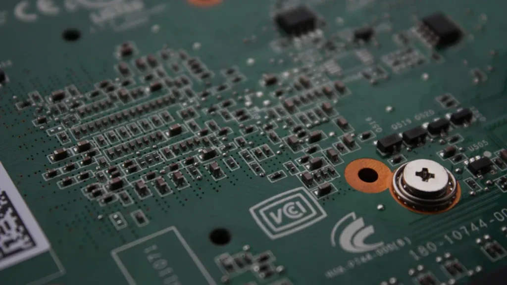
SMT PCBA uses surface mount technology to assemble electronic components directly onto pcba. This method increases efficiency and allows for compact device designs. Unlike traditional through-hole assembly, surface mounting technology attaches components to the board surface. You see its impact in modern devices like smartphones and tablets, where you benefit from smaller, more powerful designs:
- Components fit tightly, making devices slimmer.
- More features are integrated into a limited space.
- Performance and energy efficiency improve.
The SMT assembly process includes design, solder paste printing, pick and place, reflow soldering, inspection, and testing. Advanced SMT lines ensure consistent quality and speed.
What Is SMT PCBA?
- SMT PCBA allows for compact and efficient designs, making devices like smartphones and tablets smaller and more powerful.
- The SMT assembly process includes critical steps such as design, solder paste printing, and inspection, ensuring high-quality results.
- Automated processes in SMT PCBA increase production speed and reduce costs, making it a preferred choice for modern electronics.
- Understanding the differences between SMT and traditional through-hole technology helps in selecting the right assembly method for your needs.
- Future trends in SMT, like Mini-LED and HDI boards, promise even smaller and faster devices, driving innovation in electronics.
SMT PCBA and Surface Mount Technology
What Is Surface Mount Technology?
Surface mount technology refers to the process of mounting electronic components directly onto the surface of a printed circuit board. You benefit from this approach because it streamlines the SMT assembly and enables compact, high-performance devices. The table below highlights the fundamental principles that drive surface mounting technology in electronics manufacturing:
| Principle/Advantage | Description |
|---|---|
| Direct Mounting | Components attach directly to the PCB surface, increasing design flexibility. |
| Increased Component Density | More components fit in a smaller area, resulting in lighter, smaller devices. |
| Automation and Cost Reduction | Automated processes improve speed and lower labor costs. |
| Improved Performance | Shorter signal paths boost device performance. |
What Is SMT PCBA?
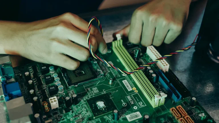
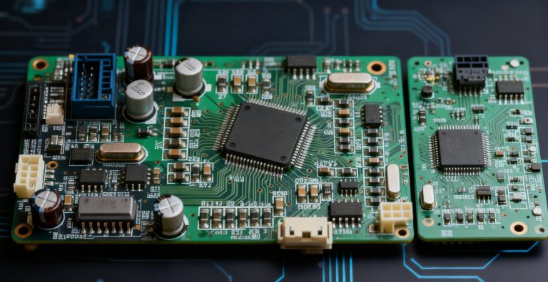
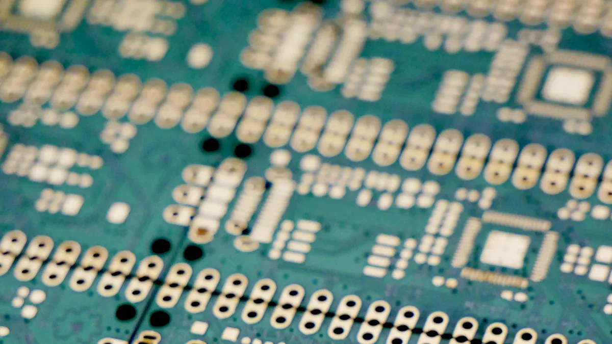
SMT PCBA describes the complete process of assembling a PCBA using surface mount technology. You see this method in modern electronics, where manufacturers use automated equipment to place and solder components. SMT PCBA allows you to achieve greater component density, efficient use of board space, and reliable performance. This approach supports the miniaturization of devices and enables advanced features in products like smartphones and industrial controllers.
SMT vs. Through-Hole Technology
You may wonder how SMT PCBA compares to traditional through-hole technology. The table below outlines key differences:
| Aspect | SMT (Surface Mount Technology) | Through-Hole Assembly |
|---|---|---|
| Component Density | Higher, with smaller footprints | Lower, larger components |
| Assembly Process | Automated, using pick-and-place machines | Manual or semi-automated, requires drilling |
| Space Utilization | Both sides of the PCB | Usually, one side only |
| Mechanical Strength | Less suitable for high-stress | Superior for connectors and power parts |
| Manufacturing Speed | Much faster throughput | Slower due to manual steps |
| High-Frequency Performance | Better due to short leads | Longer leads can introduce noise |
SMT PCBA enables you to fit more components in a smaller area, making devices lighter and more powerful. Through-hole technology offers stronger mechanical connections, which you may prefer for high-stress environments.
SMT vs. SMD: Key Differences
You often see the terms SMT and SMD used together, but they serve different roles. SMT refers to the process of mounting components onto a PCB, while SMD describes the actual components placed on the board. SMT PCBA uses SMDs to achieve higher component density and efficient assembly, which is essential for modern electronics. You rely on SMT for the assembly process and SMDs for the physical parts that make up your device.
SMT Assembly Process Steps
Surface mount technology has transformed the way you approach printed circuit board assembly. The SMT manufacturing process consists of several critical steps, each designed to maximize efficiency, quality, and compactness. Here is a detailed, step-by-step guide to the SMT assembly process:
PCB Design and SMD Selection
You begin with the design of the printed circuit board and the selection of surface-mount devices. The choice of SMD components directly affects the performance and reliability of your PCBAs.
- Electrical characteristics such as impedance, capacitance, and thermal resistance must match your design requirements to ensure stable operation.
- For high-speed designs, careful component selection maintains signal integrity and prevents noise or signal loss.
- Components with low power consumption extend battery life in portable devices.
- Thermal management is essential; components that generate heat require proper dissipation to avoid overheating.
| Standard Organization | Description |
|---|---|
| IPC | Governs PCB design, fabrication, assembly, and testing. |
| ISO | Covers manufacturing and quality control. |
| IEC | Focuses on safety and performance standards. |
| UL | Qualifies products for electrical safety. |
| ASME | Provides design and reliability standards. |
| MIL-PRF | Applies mechanical performance standards for military electronics. |
| MIL-STD | Defines requirements for military hardware. |
You should use professional design software to optimize component placement, trace routing, and thermal control. This step sets the foundation for high-density, reliable printed circuit board assembly.
Solder Paste Printing and Stencils
The next step in the SMT manufacturing process involves applying solder paste to the pcb using a stencil.
- Solder paste contains alloy powder, which forms the solder joints during reflow soldering.
- Lead-free solder paste is common due to environmental regulations, but it requires precise temperature control.
- Stencil design is crucial for accurate solder paste deposition. A well-designed stencil ensures the correct amount of paste, leading to strong and consistent joints.
- Stencil thickness, aperture design, and area ratio all influence the quality of solder paste application.
Tip: Poor stencil design can cause defects like insufficient paste, bridging, or uneven deposits, which may require costly rework.
Solder Paste Inspection (SPI)
After printing, you inspect the solder paste using automated SPI systems.
- SPI measures solder paste volume, height, area, and alignment on each pad.
- Consistent solder paste application is vital for reliable bonding and prevents defects such as shorts or weak connections.
| Metric | Description | Importance |
|---|---|---|
| Solder Paste Volume | Amount of paste on each pad | Ensures strong joints, prevents bridging |
| Solder Paste Height | Thickness of paste deposit | Maintains reliable bonding |
| Solder Paste Area | Coverage of the pad by paste | Prevents poor soldering due to insufficient coverage |
| Solder Paste Alignment | Positioning accuracy of the paste on the pad | Prevents misalignment and defective connections |
Automated SPI systems use AI and machine vision to improve defect detection rates, reducing false positives and ensuring high-quality pcb assembly.
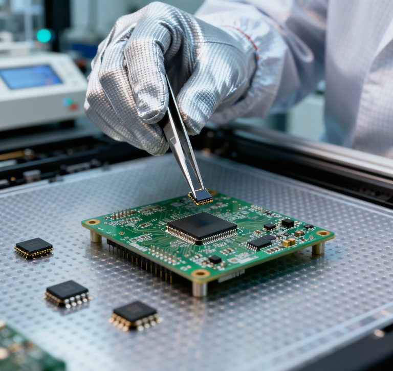
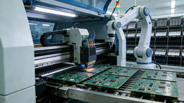
Pick and Place Machine Operation
You use high-speed pick and place machines to position SMD components onto the pcb.
- Modern machines achieve placement accuracy as tight as ±0.025 mm, ensuring perfect alignment with solder pads.
- Advanced systems use verification cameras and fine-motion adjustments for precision.
- High-speed models can place tens of thousands of components per hour, dramatically increasing throughput in SMT PCBAs.
| Machine Model | Advertised Speed (CPH) | Real-World Speed (CPH) |
|---|---|---|
| RX-8 | 100,000 | 50,000 – 70,000 |
| iineo+ | 30,000 | 15,000 – 21,000 |
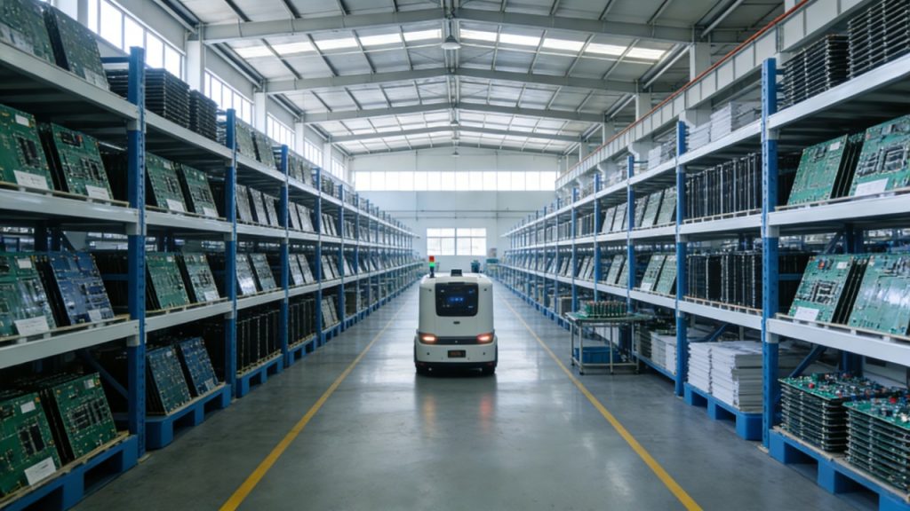
Sanshun Smart operates state-of-the-art SMT production lines with ISO 9001 certification. You benefit from turnkey PCBAs solutions focused on precision and speed, serving industries such as smart display and industrial control.
Reflow Soldering
Once components are placed, you move to reflow soldering, which bonds the SMDs to the pcb.
- The thermal profile includes preheating, soaking, peak temperature, and cooling phases.
- Lead-free solder requires higher peak temperatures (235–250 °C) compared to lead-based solder (205–220 °C).
- A gradual ramp-up and sufficient time above the melting point allow gases to escape, reducing void formation and improving joint reliability.
- The vacuum environment in advanced reflow ovens removes gases, preventing air pockets and ensuring robust, void-free solder connections.
Note: Optimizing the reflow profile is essential for producing high-reliability solder joints, especially as component density increases in modern pcba manufacturing.
AOI and X-Ray Inspection
Automated Optical Inspection (AOI) and X-ray inspection are critical for detecting assembly faults.
- AOI identifies surface-level defects such as misalignment, tombstoning, and solder bridges.
- X-ray inspection reveals hidden defects like voids, head-in-pillow, and internal solder issues.
- Combining AOI and X-ray technologies provides comprehensive defect detection, ensuring the quality and reliability of your printed circuit board assembly.
| Inspection Method | Defect Type | Detection Capability |
|---|---|---|
| AOI | Surface-level defects | Misalignment, tombstoning, solder issues |
| X-ray | Hidden defects | Voids, head-in-pillow, internal solder issues |
Final Testing and Packaging
The final step in the SMT manufacturing process involves thorough testing and secure packaging.
- Functional testing verifies that the assembled pcba operates as intended under real-world conditions.
- AOI inspection checks component placement, polarity, and solder joint quality.
- Packaging uses vacuum bags, bubble film, and moisture-proof beads to protect the PCBAs from air, moisture, and electrostatic discharge.
- A good surface finish and proper packaging extend the shelf life and reliability of your pcb assembly.
| Testing Method | Description |
|---|---|
| Functional Test (FCT) | Checks if the PCBA performs according to design specifications. |
| AOI Inspection | Uses cameras to inspect placement and solder joint quality. |
Tip: Effective packaging solutions with moisture barriers and ESD protection ensure your printed circuit board remains reliable during storage and transport.
By following these steps, you achieve efficient, high-quality, and compact SMT PCBA manufacturing. Each phase of the SMT manufacturing process supports higher component density and smaller board sizes, meeting the demands of modern electronics.
SMT PCBA Advantages and Limitations
Key Advantages of SMT PCBA
You gain significant benefits when you choose SMT PCBA for your projects. Surface mount technology enables you to design compact, high-density boards that support advanced features in modern electronics. The automated nature of the pcb assembly process allows for rapid and precise placement of components, which increases production speed and reliability. You can see the main advantages in the table below:
| Advantage | Description |
|---|---|
| Miniaturization | Ideal for compact, high-density designs where space is limited. |
| High Speed & Volume | Automated lines enable faster production and scalable throughput. |
| Cost-Effective | Streamlined assembly reduces manufacturing costs. |
| Performance | Shorter lead paths improve signal integrity and electrical performance. |
You also benefit from increased flexibility, improved reliability, and reduced manual intervention. SMT components are smaller and lighter, which allows you to fit more parts on a single pcba. This miniaturization lets you integrate more functions into smaller devices. You experience fewer issues with shock and vibration, as SMT components perform better mechanically in demanding environments.
SMT components can be reduced in volume by up to 90%, letting you achieve higher circuit density and more functionality in compact designs.
Main Limitations and Challenges
While SMT PCBA offers many advantages, you must consider several challenges during PCBA manufacturing. Specialized equipment, such as pick and place machines and reflow soldering ovens require high initial investment. Inspection becomes difficult due to the small size and number of solder joints, especially with complex packages like BGAs. You may encounter issues with fragility, as surface-mount components are more delicate than through-hole parts. Small batch production can be expensive, and power limitations restrict the use of SMT for high-heat components.
| Challenge | Description |
|---|---|
| High Initial Investment | Specialized equipment increases startup costs. |
| Difficult to Inspect | Small solder joints and fine-pitch components complicate defect detection. |
| Fragility | SMD parts are delicate and require careful handling. |
| Expensive Small-Batch Production | High setup costs make prototyping less economical. |
| Limited Power Capabilities | Not suitable for components with high heat generation. |
Environmental factors such as humidity and temperature affect solder joint integrity and overall reliability. You must control these conditions to maintain quality and reduce defects in pcb assembly.
Real-World Applications
You encounter SMT PCBA in a wide range of consumer and industrial devices. The technology supports miniaturization and high-speed circuits, making it essential for modern electronics.
- Smartphones
- Laptops
- Tablets
- Gaming consoles
- Smartwatches
- TVs
- Household appliances
- Communication devices
- Automotive control systems
- Medical diagnostic equipment
SMT PCBA enables you to build devices with advanced features, compact designs, and reliable performance across industries such as automotive, medical, and consumer electronics.
Future Trends in Surface Mounting Technology
Mini-LED and HDI Boards
You see rapid innovation in SMT PCBA as manufacturers adopt Mini-LED and high-density interconnect (HDI) boards. These technologies drive the evolution of surface mount technology, enabling you to design smaller, faster, and more reliable devices. HDI boards allow you to reduce PCB size by up to 50%, which is essential for portable electronics. Mini-LED assembly supports advanced display applications, delivering higher brightness and energy efficiency.
| Benefit | Description |
|---|---|
| Smaller Form Factors | HDI technology enables up to 30-50% reduction in PCB size, crucial for portable devices. |
| Enhanced Performance | Shorter signal paths and reduced EMI improve speed and reliability, supporting high data rates. |
| Cost Efficiency in the Long Run | Reduced material usage and improved product longevity can lower overall expenses. |
| Greater Design Flexibility | Higher layer counts and denser routing allow for innovative designs without space constraints. |
You benefit from these advancements by achieving greater component density and improved signal integrity. The PCB assembly process now supports more complex layouts, which helps you meet the demands of next-generation electronics.
The global surface mount technology market is projected to reach $8,222 million by 2030, with a compound annual growth rate of 5.8% from 2023 to 2030. You can expect continued expansion as industries invest in advanced SMT lines and automation.
Industry Applications
You encounter SMT PCBA in a wide range of industries, each driving innovation in surface mounting technology. Medical devices rely on compact, reliable PCB assembly for products like pacemakers and glucose monitors. Automotive systems use SMT lines for advanced features such as cruise control and electric vehicle battery management. Aerospace and defense applications demand high-performance, ruggedized electronics built with precision SMT processes.
| Industry Application | Examples of SMT Applications |
|---|---|
| Medical Devices | Pacemakers, Hearing Aids, and Glucose Monitors |
| Automotive | Cruise Control, Automatic Emergency Braking, Electric Vehicle Battery Management Systems |
| Aerospace and Defence | GPS Satellites, Radar Technology, Electronic Warfare Systems |
| Telecommunications | Modems, Wi-Fi Routers, Set-Top Boxes |
| Consumer Electronics | Smartphones, Laptops, Tablets, Wearables |
You see surface mount technology shaping the future of electronics in every sector. As you adopt new SMT PCBA solutions, you gain access to higher performance, miniaturization, and reliability for your products.
PCBA and SMT Terms Glossary
You often encounter specialized terms in the SMT PCBA industry. This glossary helps you understand the language used in the PCB assembly process and SMT line operations.
Surface Mount Technology (SMT)
Surface Mount Technology refers to the method you use to mount electronic components directly onto the surface of a printed circuit board. SMT enables you to achieve higher component density and supports automated assembly. You rely on SMT for efficient, compact device designs.
Surface Mount Device (SMD)
A Surface Mount Device is any electronic component designed for placement on the surface of a PCB. SMDs include resistors, capacitors, integrated circuits, and LEDs. You select SMDs to maximize space and performance in your SMT PCBA projects.
SMT Assembly
SMT Assembly describes the complete process of placing and soldering SMDs onto a PCB using automated equipment. You follow steps such as solder paste printing, pick and place machine operation, reflow soldering, and AOI inspection. SMT assembly streamlines production and improves quality.
Pick and Place Machine
A Pick and Place Machine is an automated device you use to position SMDs onto the PCB with high speed and accuracy. This machine reads design files and places thousands of components per hour. You depend on pick and place machines for precision in the SMT line.
Reflow Soldering
Reflow Soldering is the process you use to bond SMDs to the PCB by heating solder paste until it melts and forms strong joints. You control the thermal profile to ensure reliable connections. Reflow soldering is essential for modern SMT PCBA manufacturing.
AOI Inspection
Automated Optical Inspection (AOI) uses cameras and software to check for defects in the PCB assembly process. You use AOI inspection to detect misalignment, solder bridges, and missing components. AOI improves quality and reduces manual errors in the SMT line.
Through-Hole Technology (THT)
Through-Hole Technology is a traditional method where you insert component leads through holes in the PCB and solder them on the opposite side. You may choose THT for parts that require strong mechanical support. THT is less common in high-density SMT PCBA designs.
Tip: Understanding these terms helps you communicate effectively with suppliers and engineers during the PCB assembly process.
You now understand how surface mount technology shapes the way you design and build modern electronics. By following each step in the assembly process, you achieve compact, reliable, and high-performance results. SMT PCBA supports the miniaturization and complexity required in today’s devices. When you need consistent quality and advanced features, consider working with professional assembly partners to bring your next project to life.
FAQ
What is the main advantage of SMT PCBA over traditional assembly?
You achieve higher component density and faster production with SMT PCBA. Surface Mount Technology allows you to design smaller, lighter devices. Automated SMT lines increase speed and reduce manual errors.
How does a Pick and Place machine improve the PCB assembly process?
You use Pick and Place machines to position SMDs quickly and accurately. These machines read design files and place thousands of components per hour, improving efficiency and consistency in the SMT line.
Why is AOI inspection important in SMT PCBA?
You rely on AOI inspection to detect defects like misalignment and solder bridges. Automated Optical Inspection ensures quality and reduces manual errors during the PCB assembly process.
What role does reflow soldering play in SMT PCBA?
You use reflow soldering to bond SMDs to the PCB. Controlled heating melts solder paste, forming strong joints. This step is essential for reliable connections in Surface Mount Technology.
Can SMT PCBA support high-power components?
You may find SMT PCBA less suitable for high-power components. Surface-mount devices are more fragile and have limited heat dissipation compared to through-hole parts.